Built in Potential in Pn Junction Diode
This is a short video on solved problem related to PN Junction Diode. The built-in potential of a P N junction diode is 07 V at room temperature.

Pn Junction Theory For Semiconductor Diodes
Assume In 2 07.

. The two semiconductor-conductor junctions form Schottky barriers which cancel the built-in potential exactly. With Na and Nd being the acceptor donor doping in the p-region. It can be seen that Vbi is purely function of Temperature and Doping and independent of the external bias.
Temperature Biased voltage Doping density The built-in potential of p-n junction diode is a function ofaTemperaturebBiased voltagecDoping densitydNone of the aboveCorrect answer is option ABC. A pn junction diode allows electric charges to flow in one direction but not in the opposite direction. This potential difference is called built-in potential.
When the diode is connected to the voltmeter there are three junctions in total. V 0 V t l n N d N a n i 2 This equation is what I missed. I started writing a long answer and for some reason interaction between phone app and web app pc losing connection it got lost.
SOLUTION The built-in potential is given by Equation. Ad Order Batteries Battery Holders Other Parts at Digi-Key. The built in potential or barrier potential for pn junctions is given by following relation Vbi Vt ln NaNdni² which is normally of the order of 06V to 08 V.
Formation of potential of p-n junction diode depends on temperature biased voltage and doping densityThe correct answers are. Assuming you know algebra you can easily express the built in voltage in terms of the acceptor and donor concentrations. P p N A N D.
E o V T l n N D N A n i 2 where. This question was previously asked in. EXAMPLE 61 THE BUILT-IN POTENTIALS FOR Ge Si InP AND GaAs pn JUNCTIONS A pn junction diode has a concentration of 10 acceptor atoms cm on the p-side and a concentration of 107 donor atoms cm-- on the n-side.
When the p-n junction diode is in forwarding bias the p-type is linked to the positive terminal of the external voltage while the n-type is connected to the negative. What will be the approximate value of built-in potential if the doping concentrations on both sides are doubled. Edited Aug 18 2016 at 1606.
At the junction some of the free electrons. The diode is thought to be in the forward bias state if the applied voltage reduces the width of the depletion layer and reverse. This built in potential exists in the absence of any external voltage applied and no current is generated as a result of this potentialThis value is in.
What will be the built-in potential for the semiconductor materials. Two semiconductor-conductor junctions at the two ends and the pn junction. Negative charges electrons can easily flow through the junction from n to p but not from p to n and the reverse is true for holes.
Therefore the voltage reading will be 0 across a diode. The p-n junction formula which is based on the built-in potential difference generated by the electric field is as follows. The p-n junction diode characteristics and operation is closely connected to the behaviour of the carriers in the junction formed at the boundary between the p-type and n-type materials.
At the same time there was an answer from another guy and its also gone Long story short. Im very sad I have to start all over again. The electric potential between P and N-regions changes when an external potential is supplied to the PN junction terminals.
As a result the flow of the majority of carriers is altered allowing electrons and holes to diffuse through the PN junction.
What Is The Value Of Voltage At Depletion Region Of P N Junction Diode Quora
Pn Junction Theory For Semiconductor Diodes
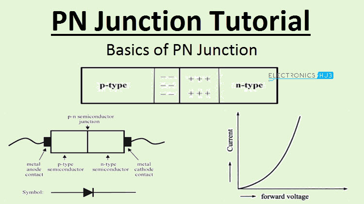
Pn Junction Tutorial Introduction To Pn Junction Diodes

Pn Junction Diode And Diode Characteristics
0 Response to "Built in Potential in Pn Junction Diode"
Post a Comment